Silicon Carbide Epitaxial Wafer Market Analysis from 2022 to 2034 Containing Market Size, Share along with its CAGR, Forecast and Trends
Top Countries — Revenue
Access the full forecast model.
Country-level data · Company profiles · Editable dataset · Analyst consultation included.
Silicon Carbide Epitaxial Wafer Market Analysis — Presence
Geographical Analysis
Click countries to exploreRegional and Country Analysis
Global Silicon Carbide Epitaxial Wafer Market Analysis 2026
| Region / Country | 2021 (A) | 2025 (A) | 2033 (P) | CAGR |
|---|---|---|---|---|
| Global | xxxx | xxxx | xxxx | 21.2% |
| North America | xxxx | xxxx | xxxx | 19.4% |
| United States | xxxx | xxxx | xxxx | xxxx |
| Canada | xxxx | xxxx | xxxx | xxxx |
| Mexico | xxxx | xxxx | xxxx | xxxx |
| Europe | xxxx | xxxx | xxxx | 19.7% |
| United Kingdom | xxxx | xxxx | xxxx | xxxx |
| France | xxxx | xxxx | xxxx | xxxx |
| Germany | xxxx | xxxx | xxxx | xxxx |
| Italy | xxxx | xxxx | xxxx | xxxx |
| Russia | xxxx | xxxx | xxxx | xxxx |
| Spain | xxxx | xxxx | xxxx | xxxx |
| Sweden | xxxx | xxxx | xxxx | xxxx |
| Denmark | xxxx | xxxx | xxxx | xxxx |
| Switzerland | xxxx | xxxx | xxxx | xxxx |
| Luxembourg | xxxx | xxxx | xxxx | xxxx |
| Rest of Europe | xxxx | xxxx | xxxx | xxxx |
| Asia Pacific | xxxx | xxxx | xxxx | 23.2% |
| China | xxxx | xxxx | xxxx | xxxx |
| Japan | xxxx | xxxx | xxxx | xxxx |
| South Korea | xxxx | xxxx | xxxx | xxxx |
| India | xxxx | xxxx | xxxx | xxxx |
| Australia | xxxx | xxxx | xxxx | xxxx |
| Singapore | xxxx | xxxx | xxxx | xxxx |
| Taiwan | xxxx | xxxx | xxxx | xxxx |
| South East Asia | xxxx | xxxx | xxxx | xxxx |
| Rest of APAC | xxxx | xxxx | xxxx | xxxx |
| South America | xxxx | xxxx | xxxx | 20.6% |
| Brazil | xxxx | xxxx | xxxx | xxxx |
| Argentina | xxxx | xxxx | xxxx | xxxx |
| Colombia | xxxx | xxxx | xxxx | xxxx |
| Peru | xxxx | xxxx | xxxx | xxxx |
| Chile | xxxx | xxxx | xxxx | xxxx |
| Rest of South America | xxxx | xxxx | xxxx | xxxx |
| Middle East | xxxx | xxxx | xxxx | 20.9% |
| Saudi Arabia | xxxx | xxxx | xxxx | xxxx |
| Turkey | xxxx | xxxx | xxxx | xxxx |
| UAE | xxxx | xxxx | xxxx | xxxx |
| Egypt | xxxx | xxxx | xxxx | xxxx |
| Qatar | xxxx | xxxx | xxxx | xxxx |
| Rest of Middle East | xxxx | xxxx | xxxx | xxxx |
| Africa | xxxx | xxxx | xxxx | xxxx |
| East Africa | xxxx | xxxx | xxxx | xxxx |
| West Africa | xxxx | xxxx | xxxx | xxxx |
| North Africa | xxxx | xxxx | xxxx | xxxx |
| South Africa | xxxx | xxxx | xxxx | xxxx |
A = Actual · E = Estimated · P = Projected · 🔒 Locked values require full access. Click headers to sort.
Unlock full regional dataset →Segmentation Analysis
Type Segment Analysis According to Cognitive Market Research, 4 inch wafers held the major market share over the forecast period. These wafers offer a balanced combination of cost-effectiveness and production efficiency, making them a preferred choice for various applications. Additionally, as semiconductor manufacturers continue to optimize production processes and enhance yield rates for 4-inch wafers, their market share is expected to remain dominant over the forecast period, driven by sustained demand across multiple industries. 6-inch wafers are the fastest-growing category over the forecast period. Advancements in manufacturing technology have significantly improved the scalability and cost-effectiveness of producing 6-inch wafers, attracting increased adoption from semiconductor manufacturers. Additionally, the larger wafer size allows for higher device density and improved manufacturing efficiency, catering to the growing demand for high-performance semiconductor devices in applications such as power electronics, automotive, and telecommunications, thereby driving the rapid growth of the 6-inch wafer segment. 2 Inch Wafers 4 Inch Wafers 6-Inch Wafers Others
Disclaimer: The charts and graphs are for illustrative purposes only and do not represent actual market values. To access accurate quantitative data, please request a paid report or request free sample.
To learn more about market share and segmentation, request the free sample pages.
Competitor Analysis
Competitive Landscape of the Silicon Carbide Epitaxial Wafer Market
The competitive landscape of the silicon carbide epitaxial wafer market is characterized by intense rivalry among manufacturers striving to innovate and improve production processes. Companies focus on enhancing product quality, expanding manufacturing capabilities, and securing partnerships to strengthen their market position amid evolving industry dynamics and customer demands.
- In August 2021, Cree Inc., along with its Wolfspeed arm, and STMicroelectronics announced an extension of their ongoing silicon carbide wafer supply agreement. The amended contract entails Cree furnishing ST with 150mm silicon carbide bare and epitaxial wafers over several years, now valued at over $800 million. This expansion fortifies ST's global silicon carbide substrate supply, aligning with their strategy to meet burgeoning demand across automotive and industrial sectors, with numerous high-volume customer programs already underway or in the pipeline.
| Top Companies (In no particular order) | 2022 (A) | 2023 (A) | 2024 (A) | 2025 (A) |
|---|---|---|---|---|
| Coherent Corp. (II-VI Incorporated) | ••• | ••• | ••• | ••• |
| Cree Inc | ••• | ••• | ••• | ••• |
| Mitsubishi Electric Corporation | ••• | ••• | ••• | ••• |
| Resonac Holdings Corporation | ••• | ••• | ••• | ••• |
| ROHM Semiconductor | ••• | ••• | ••• | ••• |
| STMicroelectronics (Norstel AB) | ••• | ••• | ••• | ••• |
| Toshiba Corporation | ••• | ••• | ••• | ••• |
| United Silicon Carbide Inc. | ••• | ••• | ••• | ••• |
| Wolfspeed Inc. | ••• | ••• | ••• | ••• |
| Xiamen Powerway Advanced Material Co. | ••• | ••• | ••• | ••• |
We Provide Regional Breakdown of this Companies and Company specific to any Country, Region, Product/ service as well. We cover market share analysis for publicly listed companies as well as privately held companies, subject to data availability.
Request company profile for validation →Report Scope & Analysis
According to Cognitive Market Research, the global silicon carbide epitaxial wafer market size is USD 815.2 million in 2024 and will expand at a compound annual growth rate (CAGR) of 21.20% from 2024 to 2031.
- North America held the major market of around 40% of the global revenue with a market size of USD 326.08 million in 2024 and will grow at a compound annual growth rate (CAGR) of 19.4% from 2024 to 2031.
- Europe accounted for a share of over 30% of the global market size of USD 244.56 million.
- Asia Pacific held the market of around 23% of the global revenue with a market size of USD 187.50 million in 2024 and will grow at a compound annual growth rate (CAGR) of 23.2% from 2024 to 2031.
- Latin America market of around 5% of the global revenue with a market size of USD 40.76 million in 2024 and will grow at a compound annual growth rate (CAGR) of 20.6% from 2024 to 2031.
- Middle East and Africa held the major market of around 2% of the global revenue with a market size of USD 16.30 million in 2024 and will grow at a compound annual growth rate (CAGR) of 20.9% from 2024 to 2031.
- The sales of 4 Inch wafers are poised to increase due to their optimal balance between manufacturing cost and device yield, making them the preferred choice for mass production in various applications.
- The sales of power devices are expected to surge due to the escalating demand for energy-efficient solutions in electric vehicles, renewable energy systems, and industrial automation, driving adoption across diverse industries.
Introduction of the Silicon Carbide Epitaxial Wafer Market
A silicon carbide epitaxial wafer refers to a crystalline substrate crucial in semiconductor manufacturing, particularly for power electronics and optoelectronic devices. These wafers are grown through epitaxial deposition techniques, wherein a single-crystal silicon carbide layer is precisely grown atop a silicon carbide substrate. This process allows for the creation of highly pure and tailored semiconductor materials with superior electrical properties, including high breakdown voltage, thermal conductivity, and efficiency at high temperatures. Silicon carbide epitaxial wafers serve as the foundation for producing advanced electronic components like high-power transistors, diodes, and sensors, enabling applications in renewable energy, electric vehicles, aerospace, and telecommunications.
Advancements in power electronics are poised to significantly boost sales of silicon carbide epitaxial wafers. As the demand for higher efficiency, lower energy consumption, and increased power density intensifies across various sectors like automotive, renewable energy, and industrial automation, silicon carbide emerges as a key enabler. Its superior electrical properties allow for the development of more efficient and compact power devices capable of handling higher voltages and temperatures. This, coupled with ongoing research and development efforts to improve manufacturing processes and reduce costs, positions silicon carbide epitaxial wafers as essential components driving the next wave of innovation in power electronics.
- In December 2023, Coherent Corp. finalized a $1 billion collective investment by Denso Corporation and Mitsubishi Electric Corporation into its silicon carbide semiconductor venture. Each company contributed $500 million, securing a 12.5% non-controlling stake in the venture, while Coherent retains the remaining 75%.
Analyst Conclusion
Author's Say's, Between 2023 and 2030, The global silicon carbide epitaxial wafer market will expand significantly by 21.20% CAGR between 2024 to 2031.
- The sales of 4-inch wafers are poised to increase due to their optimal balance between manufacturing cost and device yield, making them the preferred choice for mass production in various applications.
- The sales of power devices are expected to surge due to the escalating demand for energy-efficient solutions in electric vehicles, renewable energy systems, and industrial automation, driving adoption across diverse industries.
- The sublimation sandwich method held the highest silicon carbide epitaxial wafer market revenue share in 2024.

Kalyani Raje is a distinguished research leader and the Co-Founder & Chief Research Officer at Cognitive Market Research and Consulting, a global market research and consulting firm specializing in data-driven intelligence and strategic business insights. With over a decade of experience in market research, competitive intelligence, and analytical consulting, she has played a pivotal role in helping organizations understand evolving market landscapes and make informed strategic decisions across industries including FMCG, IT, Telecom, Automotive, Electronics, Healthcare, and Consumer Goods.
As a research professional, Kalyani is recognized for her expertise in developing rigorous research methodologies, interpreting complex market data, and transforming insights into actionable business strategies. Her analytical approach, combined with a strong understanding of global industry trends and consumer behavior, has enabled enterprises, manufacturers, investors, and business leaders to navigate competitive environments with greater confidence and clarity.
Kalyani is an active member of ESOMAR and the Market Research Society of India (MRSI), reflecting her commitment to maintaining ethical, transparent, and internationally recognized research standards. She strongly advocates adherence to the ICC/ESOMAR International Code on Market and Social Research, reinforcing her dedication to research integrity, data quality, and responsible business practices within the global insights industry.
In 2026, Kalyani was invited as a Speaker at ESOMAR Africa 2026, where she shared her expertise on Africa’s Youthquake: Decoding the Continent’s Largest Generation and Its Transformative Impact. Her participation highlighted her thought leadership in understanding demographic shifts, emerging markets, and the evolving role of data and analytics in shaping future business opportunities.
Throughout her professional journey, Kalyani has been instrumental in driving research excellence, mentoring analytical teams, and building scalable research frameworks that deliver high-value intelligence to global clients. Her passion for innovation, strategic thinking, and evidence-based decision-making continues to strengthen Cognitive Market Research’s position as a trusted global insights partner for businesses worldwide.
Frequently Asked Questions
★ Reviews
Rate this report
Silicon Carbide Epitaxial Wafer Market Analysis — Table of Contents
- This is just a redacted sample pages of the actual deliverable report and only for representative purposes
- Charts/Graphs/Numbers/data are only for Representative purposes and do not depict actual statistics.
- The table of Contents differs according to the user License selection. Current Displayed TOC is for the Corporate User License Report Edition. TOC Customization options: Add or Remove section/s Or chapter/s from the report.
- Specific Tables, Graphs, Sections, and Chapters can be ordered at a discounted price.
- If applicable; On Request Volume Data will also be provided (at an Additional Cost).
Report Scope
| Type | 2 Inch Wafers, 4 Inch Wafers, 6-Inch Wafers, Others |
|---|---|
| Application | Power Device, Electronics & Optoelectronics, Wireless Infrastructure, Others |
| Production Method | Sublimation Sandwich Method, Modified Lely Method, High-Temperature CVD, Others |
| Grade | Research, Production, Opto |
| List of Competitors | Coherent Corp. (II-VI Incorporated), Cree Inc, Mitsubishi Electric Corporation, Resonac Holdings Corporation, ROHM Semiconductor, STMicroelectronics (Norstel AB), Toshiba Corporation, United Silicon Carbide Inc., Wolfspeed Inc. , Xiamen Powerway Advanced Material Co. |
Chapter 1. Competitor Analysis (Subject to Data Availability (Private Players))
- 1.1 Top Competitors Analysis
- 1.1.1 Global Silicon Carbide Epitaxial Wafer Market Analysis by Key Players
- 1.1.2 Segment Market Analysis by Key Players
- 1.1.3 Top Players Ranking 2024
- 1.1.4 New Product Launch Analysis
- 1.1.5 Industry Mergers and Acquisition Analysis
- 1.2 Company Profile (Data Subject to Availability) Sample Format
- 1.2.1 Coherent Corp. (II-VI Incorporated)
- 1.2.1.1 Company Basic Information, Manufacturing Base, Sales Area, and Competitors
- 1.2.1.2 Business Overview
- 1.2.1.3 Financials (Subject to data availability)
- 1.2.1.4 R&D Investment (Subject to data availability)
- 1.2.1.5 Product Types Specification
- 1.2.1.6 Business Strategy
- 1.2.1.7 Recent Developments
- 1.2.1.8 Management Change
- 1.2.1.9 S.W.O.T Analysis
- 1.2.2 Cree Inc
- 1.2.2.1 Company Basic Information, Manufacturing Base, Sales Area, and Competitors
- 1.2.2.2 Business Overview
- 1.2.2.3 Financials (Subject to data availability)
- 1.2.2.4 R&D Investment (Subject to data availability)
- 1.2.2.5 Product Types Specification
- 1.2.2.6 Business Strategy
- 1.2.2.7 Recent Developments
- 1.2.2.8 Management Change
- 1.2.2.9 S.W.O.T Analysis
- 1.2.3 Mitsubishi Electric Corporation
- 1.2.3.1 Company Basic Information, Manufacturing Base, Sales Area, and Competitors
- 1.2.3.2 Business Overview
- 1.2.3.3 Financials (Subject to data availability)
- 1.2.3.4 R&D Investment (Subject to data availability)
- 1.2.3.5 Product Types Specification
- 1.2.3.6 Business Strategy
- 1.2.3.7 Recent Developments
- 1.2.3.8 Management Change
- 1.2.3.9 S.W.O.T Analysis
- 1.2.4 Resonac Holdings Corporation
- 1.2.4.1 Company Basic Information, Manufacturing Base, Sales Area, and Competitors
- 1.2.4.2 Business Overview
- 1.2.4.3 Financials (Subject to data availability)
- 1.2.4.4 R&D Investment (Subject to data availability)
- 1.2.4.5 Product Types Specification
- 1.2.4.6 Business Strategy
- 1.2.4.7 Recent Developments
- 1.2.4.8 Management Change
- 1.2.4.9 S.W.O.T Analysis
- 1.2.5 ROHM Semiconductor
- 1.2.5.1 Company Basic Information, Manufacturing Base, Sales Area, and Competitors
- 1.2.5.2 Business Overview
- 1.2.5.3 Financials (Subject to data availability)
- 1.2.5.4 R&D Investment (Subject to data availability)
- 1.2.5.5 Product Types Specification
- 1.2.5.6 Business Strategy
- 1.2.5.7 Recent Developments
- 1.2.5.8 Management Change
- 1.2.5.9 S.W.O.T Analysis
- 1.2.6 STMicroelectronics (Norstel AB)
- 1.2.6.1 Company Basic Information, Manufacturing Base, Sales Area, and Competitors
- 1.2.6.2 Business Overview
- 1.2.6.3 Financials (Subject to data availability)
- 1.2.6.4 R&D Investment (Subject to data availability)
- 1.2.6.5 Product Types Specification
- 1.2.6.6 Business Strategy
- 1.2.6.7 Recent Developments
- 1.2.6.8 Management Change
- 1.2.6.9 S.W.O.T Analysis
- 1.2.7 Toshiba Corporation
- 1.2.7.1 Company Basic Information, Manufacturing Base, Sales Area, and Competitors
- 1.2.7.2 Business Overview
- 1.2.7.3 Financials (Subject to data availability)
- 1.2.7.4 R&D Investment (Subject to data availability)
- 1.2.7.5 Product Types Specification
- 1.2.7.6 Business Strategy
- 1.2.7.7 Recent Developments
- 1.2.7.8 Management Change
- 1.2.7.9 S.W.O.T Analysis
- 1.2.8 United Silicon Carbide Inc.
- 1.2.8.1 Company Basic Information, Manufacturing Base, Sales Area, and Competitors
- 1.2.8.2 Business Overview
- 1.2.8.3 Financials (Subject to data availability)
- 1.2.8.4 R&D Investment (Subject to data availability)
- 1.2.8.5 Product Types Specification
- 1.2.8.6 Business Strategy
- 1.2.8.7 Recent Developments
- 1.2.8.8 Management Change
- 1.2.8.9 S.W.O.T Analysis
- 1.2.9 Wolfspeed Inc.
- 1.2.9.1 Company Basic Information, Manufacturing Base, Sales Area, and Competitors
- 1.2.9.2 Business Overview
- 1.2.9.3 Financials (Subject to data availability)
- 1.2.9.4 R&D Investment (Subject to data availability)
- 1.2.9.5 Product Types Specification
- 1.2.9.6 Business Strategy
- 1.2.9.7 Recent Developments
- 1.2.9.8 Management Change
- 1.2.9.9 S.W.O.T Analysis
- 1.2.10 Xiamen Powerway Advanced Material Co.
- 1.2.10.1 Company Basic Information, Manufacturing Base, Sales Area, and Competitors
- 1.2.10.2 Business Overview
- 1.2.10.3 Financials (Subject to data availability)
- 1.2.10.4 R&D Investment (Subject to data availability)
- 1.2.10.5 Product Types Specification
- 1.2.10.6 Business Strategy
- 1.2.10.7 Recent Developments
- 1.2.10.8 Management Change
- 1.2.10.9 S.W.O.T Analysis
- 1.2.1 Coherent Corp. (II-VI Incorporated)
- 1.1 Top Competitors Analysis
Chapter 2. Global Silicon Carbide Epitaxial Wafer Market Analysis
- 2.1 Global Silicon Carbide Epitaxial Wafer Market Analysis
- 2.2 Global Silicon Carbide Epitaxial Wafer Market Analysis by Region
- 2.3 Global Silicon Carbide Epitaxial Wafer Market Analysis by Type
- 2.4 Global Silicon Carbide Epitaxial Wafer Market Analysis by Application
- 2.5 Global Silicon Carbide Epitaxial Wafer Market Analysis by Production Method
- 2.6 Global Silicon Carbide Epitaxial Wafer Market Analysis by Grade
- 2.7 Global Silicon Carbide Epitaxial Wafer Market Analysis by Key Players
Chapter 3. North America Silicon Carbide Epitaxial Wafer Market Analysis
- 3.1 North America Silicon Carbide Epitaxial Wafer Market Analysis
- 3.2 North America Silicon Carbide Epitaxial Wafer Market Analysis by Country
- 3.3 North America Silicon Carbide Epitaxial Wafer Market Analysis by Type
- 3.4 North America Silicon Carbide Epitaxial Wafer Market Analysis by Application
- 3.5 North America Silicon Carbide Epitaxial Wafer Market Analysis by Production Method
- 3.6 North America Silicon Carbide Epitaxial Wafer Market Analysis by Grade
- 3.7 North America Silicon Carbide Epitaxial Wafer Market Analysis by Key Players
Chapter 4. Europe Silicon Carbide Epitaxial Wafer Market Analysis
- 4.1 Europe Silicon Carbide Epitaxial Wafer Market Analysis
- 4.2 Europe Silicon Carbide Epitaxial Wafer Market Analysis by Country
- 4.3 Europe Silicon Carbide Epitaxial Wafer Market Analysis by Type
- 4.4 Europe Silicon Carbide Epitaxial Wafer Market Analysis by Application
- 4.5 Europe Silicon Carbide Epitaxial Wafer Market Analysis by Production Method
- 4.6 Europe Silicon Carbide Epitaxial Wafer Market Analysis by Grade
- 4.7 Europe Silicon Carbide Epitaxial Wafer Market Analysis by Key Players
Chapter 5. Asia Pacific Silicon Carbide Epitaxial Wafer Market Analysis
- 5.1 Asia Pacific Silicon Carbide Epitaxial Wafer Market Analysis
- 5.2 Asia Pacific Silicon Carbide Epitaxial Wafer Market Analysis by Country
- 5.3 Asia Pacific Silicon Carbide Epitaxial Wafer Market Analysis by Type
- 5.4 Asia Pacific Silicon Carbide Epitaxial Wafer Market Analysis by Application
- 5.5 Asia Pacific Silicon Carbide Epitaxial Wafer Market Analysis by Production Method
- 5.6 Asia Pacific Silicon Carbide Epitaxial Wafer Market Analysis by Grade
- 5.7 Asia Pacific Silicon Carbide Epitaxial Wafer Market Analysis by Key Players
Chapter 6. South America Silicon Carbide Epitaxial Wafer Market Analysis
- 6.1 South America Silicon Carbide Epitaxial Wafer Market Analysis
- 6.2 South America Silicon Carbide Epitaxial Wafer Market Analysis by Country
- 6.3 South America Silicon Carbide Epitaxial Wafer Market Analysis by Type
- 6.4 South America Silicon Carbide Epitaxial Wafer Market Analysis by Application
- 6.5 South America Silicon Carbide Epitaxial Wafer Market Analysis by Production Method
- 6.6 South America Silicon Carbide Epitaxial Wafer Market Analysis by Grade
- 6.7 South America Silicon Carbide Epitaxial Wafer Market Analysis by Key Players
Chapter 7. Middle East Silicon Carbide Epitaxial Wafer Market Analysis
- 7.1 Middle East Silicon Carbide Epitaxial Wafer Market Analysis
- 7.2 Middle East Silicon Carbide Epitaxial Wafer Market Analysis by Country
- 7.3 Middle East Silicon Carbide Epitaxial Wafer Market Analysis by Type
- 7.4 Middle East Silicon Carbide Epitaxial Wafer Market Analysis by Application
- 7.5 Middle East Silicon Carbide Epitaxial Wafer Market Analysis by Production Method
- 7.6 Middle East Silicon Carbide Epitaxial Wafer Market Analysis by Grade
- 7.7 Middle East Silicon Carbide Epitaxial Wafer Market Analysis by Key Players
Chapter 8. Africa Silicon Carbide Epitaxial Wafer Market Analysis
- 8.1 Africa Silicon Carbide Epitaxial Wafer Market Analysis
- 8.2 Africa Silicon Carbide Epitaxial Wafer Market Analysis by Country
- 8.3 Africa Silicon Carbide Epitaxial Wafer Market Analysis by Type
- 8.4 Africa Silicon Carbide Epitaxial Wafer Market Analysis by Application
- 8.5 Africa Silicon Carbide Epitaxial Wafer Market Analysis by Production Method
- 8.6 Africa Silicon Carbide Epitaxial Wafer Market Analysis by Grade
- 8.7 Africa Silicon Carbide Epitaxial Wafer Market Analysis by Key Players
Chapter 9. Type Analysis
- 9.1 2 Inch Wafers
- 9.1.1 Global 2 Inch Wafers Market
- 9.1.2 Global 2 Inch Wafers Market by Region
- 9.2 4 Inch Wafers
- 9.2.1 Global 4 Inch Wafers Market
- 9.2.2 Global 4 Inch Wafers Market by Region
- 9.3 6-Inch Wafers
- 9.3.1 Global 6-Inch Wafers Market
- 9.3.2 Global 6-Inch Wafers Market by Region
- 9.4 Others
- 9.4.1 Global Others Market
- 9.4.2 Global Others Market by Region
- 9.1 2 Inch Wafers
Chapter 10. Application Analysis
- 10.1 Power Device
- 10.1.1 Global Power Device Market
- 10.1.2 Global Power Device Market by Region
- 10.2 Electronics & Optoelectronics
- 10.2.1 Global Electronics & Optoelectronics Market
- 10.2.2 Global Electronics & Optoelectronics Market by Region
- 10.3 Wireless Infrastructure
- 10.3.1 Global Wireless Infrastructure Market
- 10.3.2 Global Wireless Infrastructure Market by Region
- 10.4 Others
- 10.4.1 Global Others Market
- 10.4.2 Global Others Market by Region
- 10.1 Power Device
Chapter 11. Production Method Analysis
- 11.1 Sublimation Sandwich Method
- 11.1.1 Global Sublimation Sandwich Method Market
- 11.1.2 Global Sublimation Sandwich Method Market by Region
- 11.2 Modified Lely Method
- 11.2.1 Global Modified Lely Method Market
- 11.2.2 Global Modified Lely Method Market by Region
- 11.3 High-Temperature CVD
- 11.3.1 Global High-Temperature CVD Market
- 11.3.2 Global High-Temperature CVD Market by Region
- 11.4 Others
- 11.4.1 Global Others Market
- 11.4.2 Global Others Market by Region
- 11.1 Sublimation Sandwich Method
Chapter 12. Grade Analysis
- 12.1 Research
- 12.1.1 Global Research Market
- 12.1.2 Global Research Market by Region
- 12.2 Production
- 12.2.1 Global Production Market
- 12.2.2 Global Production Market by Region
- 12.3 Opto
- 12.3.1 Global Opto Market
- 12.3.2 Global Opto Market by Region
- 12.1 Research
Chapter 13. Qualitative Analysis (Subject to Data Availability)
- 13.1 Market Drivers
- 13.2 Market Restraints
- 13.3 Market Trends
- 13.4 Market Opportunity
- 13.5 Technological Road Map (Subject to Data Availability)
- 13.6 Product Life Cycle (Subject to Data Availability)
- 13.7 Customer and Buyer Behavior Analysis
- 13.7.1 Digital Engagement, Customer Experience & Relationship Analysis
- 13.7.2 Customer Buying Behavior & Purchase Decision Analysis
- 13.7.3 Vendor Selection, Supplier Preferences & Future Demand Trends
- 13.7.4 Pricing, Affordability & Value Perception Analysis
- 13.7.5 Customer Segmentation & Demand Pattern Analysis
- 13.8 PESTEL Analysis
- 13.8.1 Political Factors
- 13.8.2 Economic Factors
- 13.8.3 Social Factors
- 13.8.4 Technological Factors
- 13.8.5 Legal Factors
- 13.8.6 Environmental Factors
- 13.9 Industrial Chain Analysis (Subject to Data Availability)
- 13.9.1 Industry Chain Analysis
- 13.9.2 Manufacturing Cost Analysis
- 13.9.3 Supply Side Analysis
- 13.9.3.1 Raw Material Analysis
- 13.9.3.2 Raw Material Procurement Analysis
- 13.9.3.3 Raw Material Price Trend Analysis
- 13.10 Porter’s Five Forces Analysis
- 13.10.1 Bargaining Power of Suppliers
- 13.10.2 Bargaining Power of Buyers
- 13.10.3 Threat of New Entrants
- 13.10.4 Threat of Substitutes
- 13.10.5 Degree of Competition
- 13.11 Patent Analysis (Subject to Data Availability)
- 13.12 ESG Analysis
- 13.13 Geopolitical Outlook
- 13.13.1 Global Power Realignment & Strategic Alliances
- 13.13.2 Geopolitical Risk Landscape & Conflict Hotspots
- 13.13.3 International Trade Relations & Market Access Environment
- 13.13.4 Regulatory & Policy Shifts Impacting Cross-Border Operations
- 13.13.5 Supply Chain Resilience, Localization & Resource Nationalism
- 13.13.6 Technology Sovereignty & Digital Geopolitics
- 13.13.7 Strategic Implications for Investment, Growth & Market Entry
- 13.14 AI & Market Transformation
- 13.14.1 Competitive Landscape Disruption & Strategic Shifts
- 13.14.2 AI-Driven Transformation of Industry Value Chain
- 13.14.3 Evolution of Business Models & Revenue Streams
- 13.14.4 AI-Driven Product, Service & Innovation Transformation
- 13.14.5 Customer Behavior, AI Adoption & Future Market Evolution
Chapter 14. TOP 10 Country Analysis
- 14.1 Country 1
- 14.2 Country 2
- 14.3 Country 3
- 14.4 Country 4
- 14.5 Country 5
- 14.6 Country 6
- 14.7 Country 7
- 14.8 Country 8
- 14.9 Country 9
- 14.10 Country 10
Chapter 15. Research Findings
- 15.1 Key Takeaways
- 15.2 Analyst Point of View
- 15.3 Assumptions and Acronyms
Chapter 16. Research Methodology and Sources
- 16.1 Primary Data Collection
- 16.1.1 Steps for Primary Data Collection
- 16.1.1.1 Identification of KOL
- 16.1.2 Backward Integration
- 16.1.3 Forward Integration
- 16.1.4 How Primary Research Help Us
- 16.1.5 Modes of Primary Research
- 16.1.1 Steps for Primary Data Collection
- 16.2 Secondary Research
- 16.2.1 How Secondary Research Help Us
- 16.2.2 Sources of Secondary Research
- 16.3 Data Validation
- 16.3.1 Data Triangulation
- 16.4 Data Representation
- 16.1 Primary Data Collection
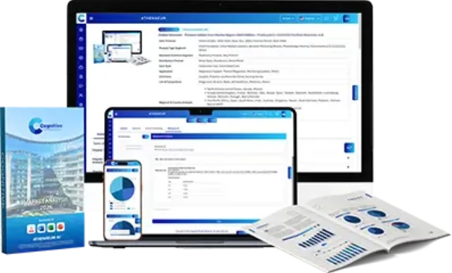
Athenaeum AI Dashboard
Our Proprietary Methodology
Cognitive Market Research and Consulting "The Full Truth" methodology — a rigorous triangulation process that combines primary research, secondary validation, and expert calibration. Implemented by Kalyani Raje and team for the Silicon Carbide Epitaxial Wafer Market Analysis Market analysis.
Primary Intelligence Gathering
Direct interviews with 50+ industry stakeholders including manufacturers, distributors, end-users, and regulatory bodies across all six regions.
Secondary Data Triangulation
Cross-referencing against trade databases, customs records, financial filings, patent databases, and verified industry publications.
Expert Validation Protocol
Each data point undergoes validation by minimum two independent domain experts with 15+ years of industry experience.
Athenaeum AI Processing
Our proprietary AI platform aggregates, normalizes, and identifies patterns across 10,000+ data points to surface non-obvious insights.
Editorial & QA Review
Final review by senior analysts ensures accuracy, coherence, and actionability of all insights and recommendations.
Data Assurance Metrics
Analytical Coverage
To maintain the integrity of our proprietary methodology and protect our elite expert network, specific source disclosures are reserved for full-access partners. Our research framework is anchored by a 70:30 primary-to-secondary ratio, ensuring your strategy is driven by real-time market intelligence rather than recycled, publicly available, or AI-generated data. Every deliverable includes an exhaustive source directory and grants direct analyst access.
Sources from the Electronics & Electrical Industry
The Three Pillars of End-to-End Market Research Services
We don't just hand over data. We partner with your team across three integrated service lines — each designed to give you decision-grade intelligence on the Silicon Carbide Epitaxial Wafer Market Analysis market.
Market Survey
Structured primary research across both B2B and B2C channels. We design and execute custom surveys targeting manufacturers, distributors, procurement heads, and end-consumers in the silicon carbide epitaxial wafer market analysis ecosystem — validated by our global panel of 10,000+ industrial respondents.
- Buyer intent & sentiment analysis
- Purchase cycle mapping
- Price sensitivity research
- Channel preference profiling
- Competitive perception study
Customized Market Data & Reports
Choose from our ready-to-access 8th Edition report or commission a fully customized dataset tailored to your exact strategic questions. Cross-splits, custom geographies, proprietary segmentation — we build the intelligence asset your board actually needs.
- Ready syndicate report
- Custom data scope & segmentation
- Excel quantitative models
- Board-ready PPT with key findings
- Secure cloud portal access
Strategic Consultation
Every survey and every report comes with dedicated analyst consultation. Our senior research team walks your leadership through findings, answers strategic questions in real-time, and helps translate data into your next board presentation or investment thesis.
- Dedicated analyst assigned to you
- Live walkthrough of findings
- Strategic Q&A sessions
- Go-to-market recommendations
- NDA-protected engagement
Customize This Report
Tell us the specific segments, regions, or companies you need — and we will tailor the deliverable to your requirements.